Web Analytics
Part Datasheet Search > Shift Registers > 74AHC595 Datasheet PDF
Images are for reference

74AHC595 Datasheet PDF

Part Series:
74AHC595 Series
Category:
Shift Registers
Description:
Shift Register Single 8Bit Serial to Serial/Parallel 16Pin SO T/R
Updated Time: 2023/01/13 02:51:07 (UTC + 8)

74AHC595 Datasheet PDF Shift Registers

23 Pages
Nexperia
IC 8Bit SRL SHFT REGIST 16-HVQFN
23 Pages
NXP
IC 8Bit SRL SHFT REGIST 16-HVQFN
23 Pages
Nexperia
IC SHIFT REGISTER 8Bit 16TSSOP
23 Pages
NXP
IC 8Bit SRL SHFT REGISTER 16SOIC
23 Pages
Nexperia
IC SHIFT REGISTER 8Bit 16DHVQFN
23 Pages
Nexperia
IC 8Bit SRL SHFT REGISTER 16SOIC
23 Pages
NXP
NPN general-purpose double transistors output latches; 3-state
23 Pages
Philips
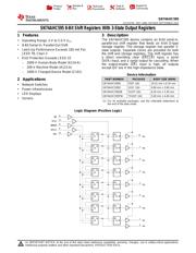
8Bit serial-in/serial or parallel-out shift register with output latches; 3-state
23 Pages
NXP
Shift Register Single 8Bit Serial to Serial/Parallel Automotive 16Pin TSSOP T/R
23 Pages
NXP
Shift Register Single 8Bit Serial to Serial/Parallel Automotive 16Pin DHVQFN EP T/R
23 Pages
Nexperia
IC SHIFT REGISTER 8Bit 16SOIC
23 Pages
NXP
NPN general-purpose double transistors output latches; 3-state
23 Pages
TI
8-Bit Shift Registers With 3-State Output Registers 16-SOIC -40 to 125
22 Pages
NXP
74AHC Series 5V 8Bit Serial-In/Serial-Out/Parallel-Out Shift Register TSSOP-16
11 Pages
Diodes
Shift Register Single 8Bit Serial to Serial/Parallel 16Pin SO T/R
10 Pages
Diodes
Logic AHC Std,TSSOP-16,T&R;,2.5K

74AHC595S16-13 - Diodes Specifications

TYPE
DESCRIPTION
Mounting Style
Surface Mount
Number of Pins
16 Pin
Case/Package
SO-16
Number of Outputs
9 Output
Number of Circuits
1 Circuit
show more

74AHC595S16-13 - Diodes Function Overview

Description
The 74AHC595 is an advanced high speed CMOS device.
An eight bit shift register accepts data from the serial input (DS) on each positive transition of the shift register clock (STCP). When asserted low the reset function (MR) sets all shift register values to zero and is independent of all clocks.
Data from the input serial shift register is placed in the output register with a rising pulse on the storages resister clock (SHCP). With the output enable (OEሻasserted low the 3-state outputs Q0-Q7 become active and present.
All registers capture data on rising edge and change output on the falling edge. If both clocks are connected together, the input shift register is always one clock cycle ahead of the output register.
Features
Wide Supply Voltage Range from 2.0 V to 5.5V
Sinks or sources 8mA at VCC= 4.5V
CMOS low power consumption
Schmitt Trigger Action at All Inputs
Inputs Accept up to 5.5V
ESD Protection Tested per JESD 22
 Exceeds 200-V Machine Model (A115-A)
 Exceeds 2000-V Human Body Model (A114-A)
 Exceeds 1000-V Charged Device Model (C101C)
Latch-Up Exceeds 250mA per JESD 78, Class II
Totally Lead-Free & Fully RoHS Compliant (Notes 1 & 2)
Halogen and Antimony Free. “Green” Device (Note 3)
Applications
General Purpose Logic
Serial to Parallel Data conversion
Capture and hold data for extended periods of time
Allow simple serial bit streams from a microcontrolle
many peripheral lines as needed
Wide array of products such as:
Computer peripherals
Appliances
Industrial control
show more
Part Datasheet PDF Search
Loading...
72,405,303 Parts Datasheet PDF, Update more than 5,000 PDF files ervery day.

Relate Parts