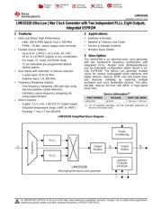
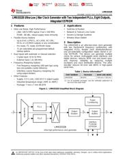
●The LMK03328 is an ultra-low-noise clock generator with two fractional-N frequency synthesizers with integrated VCOs, flexible clock distribution/fanout, and pin-selectable configuration states stored in on-chip EEPROM. The device can generate multiple clocks for various multi-gigabit serial interfaces and digital devices, reduces BOM cost and board area, and improves reliability by replacing multiple oscillators and clock distribution devices. The ultra-low-jitter reduces bit error rate (BER) in high-speed serial links.
●For each PLL, a differential/single-ended clock or crystal input can be selected as the PLL reference clock. The selected PLL reference input can be used to lock the VCO frequency at an integer or fractional multiple of the reference input frequency. The VCO frequency for the respective PLLs can be tuned between 4.8 GHz and 5.4 GHz. Both PLL/VCOs are equivalent in performance and functionality. Each PLL offers the flexibility to select a predefined or user-defined loop bandwidth, depending on the needs of the application. Each PLL has a postdivider that can be selected between divide-by 2, 3, 4, 5, 6, 7 or 8.
●All the output channels can select the divided-down VCO clock from PLL1 or PLL2 as the source for the output divider to set the final output frequency. Some output channels can also independently select the reference input for PLL1 or PLL2 as an alternative source to be bypassed to the corresponding output buffers. The 8-bit output dividers support a divide range of 1 to 256 (even or odd), output frequencies up to 1 GHz, and output phase synchronization capability.
●All output pairs are ground-referenced CML drivers with programmable swing that can be interfaced to LVDS or LVPECL or CML receivers with AC coupling. All output pairs can also be independently configured as HCSL outputs or 2× 1.8-V LVCMOS outputs. The outputs offer lower power at 1.8 V, higher performance and power supply noise immunity, and lower EMI compared to voltage-referenced driver designs (such as traditional LVDS and LVPECL drivers). Two additional 3.3-V LVCMOS outputs can be obtained via the STATUS pins. This is an optional feature in case of a need for 3.3-V LVCMOS outputs and device status signals are not needed. The device features self startup from on-chip programmable EEPROM or pre-defined ROM memory, which offers multiple custom device modes selectable via pin control and can eliminate the need for serial programming. The device registers and on-chip EEPROM settings are fully programmable via I2C-compatible serial interface. The device slave address is programmable in EEPROM and LSBs are settable with a 3-state pin.
●The device provides two frequency margining options with glitch-free operation to support system design verification tests (DVT), such as standard compliance and system timing margin testing. Fine frequency margining (in ppm) can be supported by using a low-cost pullable crystal on the internal crystal oscillator (XO), and selecting this input as the reference to the PLL synthesizer. The frequency margining range is determined by the crystal\x92s trim sensitivity and the on-chip varactor range. XO frequency margining can be controlled through pin or I2C control for ease-of-use and high flexibility. Coarse frequency margining (in %) is available on any output channel by changing the output divide value via I2C interface, which synchronously stops and restarts the output clock to prevent a glitch or runt pulse when the divider is changed.
●Internal power conditioning provide excellent power supply noise rejection (PSNR), reducing the cost and complexity of the power delivery network. The analog and digital core blocks operate from 3.3 V ± 5% supply and output blocks operate from 1.8 V / 2.5 V / 3.3 V ± 5% supply.