Web Analytics
Part Datasheet Search > - > TLC2201 Datasheet PDF
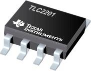
Images are for reference

TLC2201 Datasheet PDF

Part Series:
TLC2201 Series
Category:
-
Description:
Advanced LinCMOS™ LOW-NOISE PRECISION OPERATIONAL AMPLIFIERS
Updated Time: 2023/01/13 02:57:43 (UTC + 8)

TLC2201 Datasheet PDF -

70 Pages
TI
TEXAS INSTRUMENTS TLC2201AID Operational Amplifier, Single, 1 Amplifier, 1.9MHz, 2.7V/µs, ± 2.3V to ± 8V, SOIC, 8Pins
70 Pages
TI
Op Amp Single GP R-R O/P ±8V/16V 8Pin CDIP Tube
70 Pages
TI
TEXAS INSTRUMENTS TLC2201CP Operational Amplifier, Single, 1 Amplifier, 1.8MHz, 2.7V/µs, ± 2.3V to ± 8V, DIP, 8Pins
70 Pages
TI
OP Amp Single GP R-R O/P ±8V/16V 8Pin SOIC T/R
70 Pages
TI
TEXAS INSTRUMENTS TLC2201IP Operational Amplifier, Single, 1 Amplifier, 1.9MHz, 2.7V/µs, ± 2.3V to ± 8V, DIP, 8Pins
70 Pages
TI
TEXAS INSTRUMENTS TLC2201ID Operational Amplifier, Single, 1 Amplifier, 1.9MHz, 2.7V/µs, ± 2.3V to ± 8V, SOIC, 8Pins
70 Pages
TI
Op Amp Single GP R-R O/P ±8V/16V 8Pin SOIC T/R
70 Pages
TI
OP Amp Single GP R-R O/P ±8V/16V 8Pin CDIP Tube
70 Pages
TI
OP Amp Single GP R-R O/P ±8V/16V 8Pin SOIC T/R
70 Pages
TI
Operational Amplifier, Single, 1 Amplifier, 1.9MHz, 2.7V/µs, ± 2.3V to ± 8V, SOIC, 8Pins
70 Pages
TI
Op Amp Single GP R-R O/P ±8V/16V 8Pin SOIC T/R
70 Pages
TI
Op Amp Single GP R-R O/P ±8V/16V 8Pin SOIC T/R
70 Pages
TI
OP Amp Single GP R-R O/P ±8V/16V 20Pin CLLCC Tube
70 Pages
TI
Operational Amplifier, Single, 1 Amplifier, 1.8MHz, 2.5V/µs, ± 2.3V to ± 8V, SOIC, 8Pins
70 Pages
TI
TEXAS INSTRUMENTS TLC2201CDG4 Operational Amplifier, Single, 1 Amplifier, 1.9MHz, 2.7V/µs, ± 2.3V to ± 8V, SOIC, 8Pins
70 Pages
TI
Advanced LinCMOS™ LOW-NOISE PRECISION OPERATIONAL AMPLIFIERS

TLC2201 Specifications

TYPE
DESCRIPTION
Case/Package
PDIP-8
show more

TLC2201 Function Overview

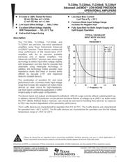
The TLC220x, TLC220xA, TLC220xB, and TLC220xY are precision, low-noise operational amplifiers using Texas Instruments Advanced LinCMOS™ process. These devices combine the noise performance of the lowest-noise JFET amplifiers with the dc precision available previously only in bipolar amplifiers. The Advanced LinCMOS™ process uses silicon-gate technology to obtain input offset voltage stability with temperature and time that far exceeds that obtainable using metal-gate technology. In addition, this technology makes possible input impedance levels that meet or exceed levels offered by top-gate JFET and expensive dielectric-isolated devices.
The combination of excellent DC and noise performance with a common-mode input voltage range that includes the negative rail makes these devices an ideal choice for high-impedance, low-level signal-conditioning applications in either single-supply or split-supply configurations.
The device inputs and outputs are designed to withstand –100-mA surge currents without sustaining latch-up. In addition, internal ESD-protection circuits prevent functional failures at voltages up to 2000 V as tested under MIL-PRF-38535, Method 3015.2; however, care should be exercised in handling these devices as exposure to ESD may result in degradation of the parametric performance.
The C-suffix devices are characterized for operation from 0°C to 70°C. The I-suffix devices are characterized for operation from –40°C to 85°C. The M-suffix devices are characterized for operation over the full military temperature range of –55°C to 125°C.
B Grade Is 100% Tested for Noise
30 nV/Hz Max at f = 10 Hz
12 nV/Hz Max at f = 1 kHz
Low Input Offset Voltage . . . 500 µV Max
Excellent Offset Voltage Stability With Temperature . . . 0.5 µV/°C Typ
Rail-to-Rail Output Swing
Low Input Bias Current
1 pA Typ at TA = 25°C
Common-Mode Input Voltage Range Includes the Negative Rail
Fully Specified For Both Single-Supply and Split-Supply Operation
Advanced LinCMOS is a trademark of Texas Instruments Incorporated.
All other trademarks are the property of their respective owners.
show more
Part Datasheet PDF Search
Loading...
72,405,303 Parts Datasheet PDF, Update more than 5,000 PDF files ervery day.
Relate Parts