Part Datasheet Search > - > TLC274 Datasheet PDF
Images are for reference
TLC274 Datasheet PDF
Part Series:
TLC274 Series
Category:
-
Description:
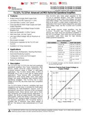
The TLC274 and TLC279 quad operational amplifiers combine a wide range of input offset voltage grades with low offset voltage drift, high input impedance, low noise, and speeds approaching that of general-purpose BiFET devices
Document:
Updated Time: 2023/01/13 01:48:00 (UTC + 8)
TLC274 - Datasheet PDF
TLC274 Datasheet PDF -
65 Pages
TI
Standard Linear AmplifierQuad Single Supply Operational Amplifier OP Amp Quad GP 16V 14Pin TSSOP T/R
53 Pages
TI
TEXAS INSTRUMENTS TLC274CD Operational Amplifier, Quad, 4 Amplifier, 1.3MHz, 3.6V/µs, 3V to 16V, SOIC, 14Pins
53 Pages
TI
TEXAS INSTRUMENTS TLC274CN Operational Amplifier, Quad, 4 Amplifier, 1.8MHz, 3.6V/µs, 3V to 16V, DIP, 14Pins
53 Pages
TI
TEXAS INSTRUMENTS TLC274BIDR Operational Amplifier, Quad, 4 Amplifier, 1.7MHz, 3.6V/µs, 4V to 16V, SOIC, 14Pins
53 Pages
TI
Operational Amplifier, Quad, 4 Amplifier, 1.7MHz, 3.6V/µs, 4V to 16V, SOIC, 14Pins
53 Pages
TI
TEXAS INSTRUMENTS TLC274BIN Operational Amplifier, Quad, 4 Amplifier, 1.7MHz, 3.6V/µs, 4V to 16V, DIP, 14Pins
53 Pages
TI
TEXAS INSTRUMENTS TLC274ACD Operational Amplifier, Quad, 4 Amplifier, 1.7MHz, 3.6V/µs, 3V to 16V, SOIC, 14Pins
53 Pages
TI
Standard Linear AmplifierLinCMOS(TM) Precision Quad Operational Amplifier OP Amp Quad GP 16V 14Pin PDIP Tube
53 Pages
TI
TEXAS INSTRUMENTS TLC274IN Operational Amplifier, Quad, 4 Amplifier, 1.7MHz, 3.6V/µs, 4V to 16V, DIP, 14Pins
53 Pages
TI
TEXAS INSTRUMENTS TLC274AID Operational Amplifier, Quad, 4 Amplifier, 2.6MHz, 3.6V/µs, 4V to 16V, SOIC, 14Pins
53 Pages
TI
TEXAS INSTRUMENTS TLC274BID Operational Amplifier, Quad, 4 Amplifier, 1.7MHz, 3.6V/µs, 4V to 16V, SOIC, 14Pins
53 Pages
TI
TEXAS INSTRUMENTS TLC274IPW Operational Amplifier, Quad, 4 Amplifier, 1.7MHz, 3.6V/µs, 4V to 16V, TSSOP, 14Pins
53 Pages
TI
TEXAS INSTRUMENTS TLC274BCDR Operational Amplifier, Quad, 1.7MHz, 4 Amplifier, 3.6V/µs, 3V to 16V, SOIC, 14Pins
53 Pages
TI
The TLC274 and TLC279 quad operational amplifiers combine a wide range of input offset voltage grades with low offset voltage drift, high input impedance, low noise, and speeds approaching that of general-purpose BiFET devices
Part Datasheet PDF Search
72,405,303 Parts Datasheet PDF, Update more than 5,000 PDF files ervery day.
