Web Analytics
Part Datasheet Search > Logic ICs > 74HCT595 Datasheet PDF
Images are for reference

74HCT595 Datasheet PDF

Part Series:
74HCT595 Series
Category:
Logic ICs
Description:
IC SHIFT REGISTER 8Bit 16SOIC
Updated Time: 2023/01/13 01:50:09 (UTC + 8)

74HCT595 Datasheet PDF Logic ICs

24 Pages
Nexperia
IC SHIFT REGISTER 8Bit 16TSSOP
24 Pages
Nexperia
IC SHIFT REGISTER 8Bit 16SOIC
24 Pages
NXP
Shift Register Single 8Bit Serial to Serial/Parallel 16Pin TSSOP T/R
24 Pages
Nexperia
Shift Register Single 8Bit Serial to Serial/Parallel 16Pin SO
24 Pages
Nexperia
IC SHIFT REGISTER 8Bit 16TSSOP
24 Pages
NXP
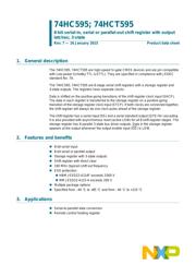
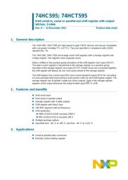
8Bit serial-in, serial or parallel-out shift register with output latches; 3-state
24 Pages
Nexperia
IC SHIFT REGISTER 8Bit 16DHVQFN
24 Pages
NXP
Shift Register Single 8Bit Serial to Serial/Parallel 16Pin SSOP Bulk
24 Pages
NXP
Shift Register Single 8Bit Serial to Serial/Parallel 16Pin DHVQFN EP T/R
24 Pages
NXP
Shift Register Single 8Bit Serial to Serial/Parallel 16Pin PDIP
23 Pages
Nexperia
IC SHIFT REGISTER 8Bit 16SOIC
23 Pages
Nexperia
IC SHIFT REGISTER 8Bit 16SOIC
23 Pages
Nexperia
IC SHIFT REGISTER 8Bit 16TSSOP
22 Pages
Nexperia
IC 8Bit SHIFT REGISTER 16-DHVQFN
12 Pages
Diodes
Logic HCT Std,SO-16,T&R;,2.5K
11 Pages
Diodes
Shift Register Single 8Bit Serial to Serial/Parallel 16Pin TSSOP T/R

74HCT595D,118 Specifications

TYPE
DESCRIPTION
Mounting Style
Surface Mount
Number of Pins
16 Pin
Case/Package
SOIC-16
Number of Outputs
9 Output
Number of Channels
8 Channel
show more

74HCT595D,118 Function Overview

The 74HCT595D is a 8-bit serial-in/serial or parallel-out Shift Register with a storage register and 3-state outputs. Both the shift and storage register have separate clocks. The device features a serial input (DS) and a serial output (Q7S) to enable cascading and an asynchronous reset MR\ input. A low on MR\ will reset the shift register. Data is shifted on the low-to-high transitions of the SHCP input. The data in the shift register is transferred to the storage register on a low-to-high transition of the STCP input. If both clocks are connected together, the shift register will always be one clock pulse ahead of the storage register. Data in the storage register appears at the output whenever the OE\ is low. A high on OE\ causes the outputs to assume a high-impedance OFF-state. Operation of the OE\ input does not affect the state of the registers. Inputs include clamp diodes.
Shift register with direct clear
100MHz Typical shift out frequency
TTL Input level
Complies with JEDEC standard No. 7A
show more
Part Datasheet PDF Search
Loading...
72,405,303 Parts Datasheet PDF, Update more than 5,000 PDF files ervery day.

Relate Parts