Web Analytics
Part Datasheet Search > Flip Flops > CD4098 Datasheet PDF
Images are for reference

CD4098 Datasheet PDF

Part Series:
CD4098 Series
Category:
Flip Flops
Description:
Monostable Multivibrator Dual -55℃ 125℃ 16Pin SOIC T/R
Updated Time: 2023/01/13 01:52:26 (UTC + 8)

CD4098 Datasheet PDF Flip Flops

17 Pages
TI
Monostable Multivibrator Dual -55℃ 125℃ 16Pin CDIP Tube
17 Pages
TI
Monostable Multivibrator Dual -55℃ 125℃ 16Pin SOIC T/R
17 Pages
TI
Monostable Multivibrator Dual -55℃ 125℃ 16Pin CDIP Tube
16 Pages
TI
Monostable Multivibrator Dual -55℃ 125℃ 16Pin SOIC T/R
16 Pages
TI
Monostable Multivibrator Dual -55℃ 125℃ 16Pin SOIC T/R
16 Pages
TI
TEXAS INSTRUMENTS CD4098BEE4 Monostable Multivibrator, CD4098, 100ns, 6.8mA, 3V to 18V, DIP-16
16 Pages
TI
TEXAS INSTRUMENTS CD4098BMG4 Monostable Multivibrator, CD4098, 100ns, 6.8mA, 3V to 18V, SOIC-16
16 Pages
TI
IC DUAL MONOSTBL MULTIVIB 16SOIC
16 Pages
TI
IC DUAL MONSTBL MULTIVIB 16TSSOP

CD4098BM96 Specifications

TYPE
DESCRIPTION
Mounting Style
Surface Mount
Number of Pins
16 Pin
Supply Voltage (DC)
3.00V (min)
Case/Package
SOIC-16
Output Current
6.80 mA
show more

CD4098BM96 Function Overview

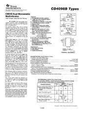
The CD4098BM96 is a CMOS dual Monostable Multivibrator provides stable retriggerable/resettable one-shot operation for any fixed-voltage timing application. An external resistor (RX) and an external capacitor (CX) control the timing for the circuit. Adjustment of RX and CX provides a wide range of output pulse widths from the Q and Q\ terminals. The time delay from trigger input to output transition (trigger propagation delay) and the time delay from set input to output transition (RESET propagation delay) are independent of RX and CX. Leading-edge-triggering (+TR) and trailing-edge-triggering (-TR) input are provided for triggering from either edge of an input pulse. An unused +TR input should be tied to VSS. An unused (-TR) input should be tied to VDD. A RESET (on low level) is provided for immediate termination of the output pulse or to prevent output pulses when power is turned on. An unused RESET input should be tied to VDD.
Retriggerable/resettable capability
Trigger and reset propagation delays independent of RX, CX
Triggering from leading or trailing edge
Separate resets
Wide range of output-pulse widths
100% Tested for maximum quiescent current at 20V
Standardized, symmetrical output characteristics
Green product and no Sb/Br
show more
Part Datasheet PDF Search
Loading...
72,405,303 Parts Datasheet PDF, Update more than 5,000 PDF files ervery day.
Relate Parts