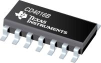
●CD4016B Series types are quad bilateral switches intended for the transmission or multiplexing of analog or digital signals. Each of the four independent bilateral switches has a single control signal input which simultaneously biases both the p and n device in a given switch on or off.
●The CD4016 "B" Series types are supplied in 14-lead hermetic dual-in-line ceramic packages (F3A suffix), 14-lead dual-in-line plastic packages (E suffix), 14-lead small-outline packages (M, MT, M96, and NSR suffixes), and 14-lead thin shrink small-outline packages (PW and PWR suffixes).
● 20-V digital or ± 10-V peak-to-peak switching
● 280- typical on-state resistance for 15-V operation
● Switch on-state resistance matched to within 10 typ. over 15-V signal-input range
● High on/off output-voltage ratio:
● 65 dB typ. @ fis = 10 kHz, RL = 10 k
● High degree of linearity:
● <0.5% distortion typ. @ fis = 1 kHz, Vis = 5 Vp-p, VDDVSS
● Extremely low off-state switch leakage resulting in very low offset current and high effective off-state resistance:
● 100pA typ. @ VDDVSS = 18 V, TA = 25°C
● Extremely high control input impedance (control circuit isolated form signal circuit:
● 1012typ.
● Low crosstalk between switches:
● 50 dB typ. @ fis= 0.9 MHz, RL = 1 k
● Matched control-input to signal-output capacitance:
● Reduces output signal transients
● Frequency response, switch on = 40MHz (typ.)
● 100% tested for quiescent current at 20 V
● Maximum control input current of 1 µA at 18 V over full package temperature range; 100 nA at 18 V and 25°C
● 5-V, 10-V, and 15-V parametric ratings
● Applications:
● Analog signal switching/multiplexing
● Signal gating
● Squelch control
● Chopper
● Modulator
● Demodulator
● Commutating switch
● Digital signal switching/multiplexing
● CMOS logic implementation
● Analog-to-digital & digital-to-analog conversion
● Digital control of frequency, impedance, phase, and analog-signal gain
●Data sheet acquired from Harris Semiconductor


