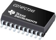
●The CD74FCT245 is an octal bus transceiver with 3-state outputs using a small-geometry BiCMOS technology. The output stages are a combination of bipolar and CMOS transistors that limit the output high level to two diode drops below VCC. This resultant lowering of output swing (0 V to 3.7 V) reduces the power-bus ringing [a source of electromagnetic interference (EMI)] and minimizes VCC bounce and ground bounce and their effects during simultaneous output switching. The output configuration also enhances switching speed and is capable of sinking 64 mA.
●The CD74FCT245 allows data transmission from the A bus to the B bus or from the B bus to the A bus, depending upon the logic level at the direction-control (DIR) input. The output-enable (OE\\) input can be used to disable the device so that the buses are effectively isolated.
●To ensure the high-impedance state during power up or power down, OE\ should be tied to VCC through a pullup resistor; the minimum value of the resistor is determined by the current-sinking capability of the driver.
●The CD74FCT245 is characterized for operation from 0°C to 70°C.
● BiCMOS Technology With Low Quiescent Power
● Buffered Inputs
● Noninverted Outputs
● Input/Output Isolation From VCC
● Controlled Output Edge Rates
● 64-mA Output Sink Current
● Output Voltage Swing Limited to 3.7 V
● SCR Latch-Up-Resistant BiCMOS Process and Circuit Design
● Package Options Include Plastic Small-Outline (M) and Shrink Small-Outline (SM) Packages and Standard Plastic (E) DIP


