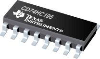
●The device is useful in a wide variety of shifting, counting and storage applications. It performs serial, parallel, serial to parallel, or parallel to serial data transfers at very high speeds.
●The two modes of operation, shift right (Q0-Q1) and parallel load, are controlled by the state of the Parallel Enable (PE)\ input. Serial data enters the first flip-flop (Q0) via the J and K\ inputs when the PE\ input is high, and is shifted one bit in the direction Q0-Q1-Q2-Q3 following each Low to High clock transition. The J and K\ inputs provide the flexibility of the JK-type input for special applications and by tying the two pins together, the simple D-type input for general applications. The device appears as four common-clocked D flip-flops when the PE\ input is Low. After the Low to High clock transition, data on the parallel inputs (D0-D3) is transferred to the respective Q0-Q3 outputs. Shift left operation (Q3-Q2) can be achieved by tying the Qn outputs to the Dn-1 inputs and holding the PE\ input low.
●All parallel and serial data transfers are synchronous, occurring after each Low to High clock transition. The HC195 series utilizes edge triggering; therefore, there is no restriction on the activity of the J, K\, Pn and PE\ inputs for logic operations, other than set-up and hold time requirements. A Low on the asynchronous Master Reset (MR)\ input sets all Q outputs Low, independent of any other input condition.
● Asynchronous Master Reset
● J, K\,(D) Inputs to First Stage
● Fully Synchronous Serial or Parallel Data Transfer
● Shift Right and Parallel Load Capability
● Complementary Output From Last Stage
● Buffered Inputs
● Typical fMAX = 50MHz at VCC = 5V, CL = 15pF, TA = 25°C
● Fanout (Over Temperature Range)
● Standard Outputs . . . . 10 LSTTL Loads
● Bus Driver Outputs . . . . 15 LSTTL Loads
● Wide Operating Temperature Range . . . 55°C to 125°C
● Balanced Propagation Delay and Transition Times
● Significant Power Reduction Compared to LSTTL Logic ICs
● HC Types
● 2V to 6V Operation
● High Noise Immunity: NIL = 30%, NIH = 30%of VCC at VCC = 5V
●Data sheet acquired from Harris Semiconductor


