Part Datasheet Search > Clock Drivers, PLLs > Cypress Semiconductor > CY7B991V5JC Datasheet PDF

$ 0
CY7B991V5JC Datasheet PDF - Cypress Semiconductor
Manufacturer:
Cypress Semiconductor
Category:
Clock Drivers, PLLs
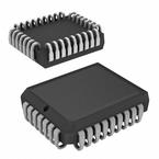
Case Package:
PLCC
Description:
IC CLK BUFFER 8:8 80MHz 32PLCC
Pictures:
3D Model
Symbol
Footprint
Pinout
Product Pictures

CY7B991V5JC Datasheet PDF (12 Pages)
Part Datasheet PDF Search
72,405,303 Parts Datasheet PDF, Update more than 5,000 PDF files ervery day.
Relate Parts
BOM Matching ToolUpload BOM File
Matching parts
Alternative parts
Warning risks
Computing costs
File format: *.xlsx, *.xls, *.csv
Online 3D Gerber ViewerUpload Gerber File
Modeling in 15s
Preview PCB
40 types of layers
Preflight Risk
Support standard RS-274X file, accept zip rar or 7z
