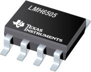
●The LMH6505 is a wideband DC coupled voltage controlled gain stage followed by a high speed current feedback operational amplifier which can directly drive a low impedance load. The gain adjustment range is 80 dB for up to 10 MHz which is accomplished by varying the gain control input voltage, VG.
●Maximum gain is set by external components, and the gain can be reduced all the way to cutoff. Power consumption is 110 mW with a speed of 150 MHz and a gain control bandwidth (BW) of 100 MHz. Output referred DC offset voltage is less than 55 mV over the entire gain control voltage range. Device-to-device gain matching is within ±0.5 dB at maximum gain. Furthermore, gain is tested and ensured over a wide range. The output current feedback op amp allows high frequency large signals (Slew Rate = 1500 V/μs) and can also drive a heavy load current (60 mA) ensured.
●Near ideal input characteristics (i.e. low input bias current, low offset, low pin 3 resistance) enable the device to be easily configured as an inverting amplifier as well.
●To provide ease of use when working with a single supply, the VG range is set to be from 0V to +2V relative to the ground pin potential (pin 4). VG input impedance is high in order to ease drive requirement. In single supply operation, the ground pin is tied to a "virtual" half supply.
●The LMH6505’s gain control is linear in dB for a large portion of the total gain control range from 0 dB down to −85 dB at 25°C, as shown below. This makes the device suitable for AGC applications. For linear gain control applications, see the LMH6503 datasheet.
●The LMH6505 is available in either the 8-Pin SOIC or the 8-Pin VSSOP package. The combination of minimal external components and small outline packages allows the LMH6505 to be used in space-constrained applications.
● VS = ±5V, TA = 25°C, RF = 1 kΩ, RG = 100Ω, RL = 100Ω, AV = AVMAX = 9.4 V/V, Typical Values Unless Specified.
● −3 dB BW 150 MHz
● Gain Control BW 100 MHz
● Adjustment Range (<10 MHz) 80 dB
● Gain Matching (Limit) ±0.50 dB
● Supply Voltage Range 7V to 12V
● Slew Rate (Inverting) 1500 V/μs
● Supply Current (No Load) 11 mA
● Linear Output Current ±60 mA
● Output Voltage Swing ±2.4V
● Input Noise Voltage 4.4 nV/√Hz
● Input Noise Current 2.6 pA/√Hz
● THD (20 MHz, RL = 100Ω, VO = 2 VPP) −45 dBc
●All trademarks are the property of their respective owners.


