Part Datasheet Search > Microcontrollers > NXP > MK60DN512ZVLQ10 Datasheet PDF
 Part 3D Model
$ 15.69
MK60DN512ZVLQ10 Datasheet PDF - NXP
Manufacturer:
NXP
Category:
Microcontrollers
Case Package:
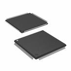
LQFP-144
Description:
MCU 32Bit ARM Cortex M4 RISC 512KB Flash 1.8V/2.5V/3.3V 144Pin LQFP Tray
Pictures:
3D Model
Symbol
Footprint
Pinout
Product Pictures
MK60DN512ZVLQ10 Datasheet PDF
AiEMA has not yet included the datasheet for MK60DN512ZVLQ10
If necessary, please send a supplementary document request to the administrator

MK60DN512ZVLQ10 Datasheet PDF (78 Pages)
MK60DN512ZVLQ10 Specifications
TYPE
DESCRIPTION
Mounting Style
Surface Mount
Frequency
100 MHz
Number of Pins
144 Pin
Supply Voltage (DC)
1.71V (min)
Operating Voltage
1.71V ~ 3.6V
Case/Package
LQFP-144
Halogen Free Status
Halogen Free
Clock Speed
100 MHz
RAM Memory Size
128 KB
Number of Bits
32 Bit
FLASH Memory Size
512 KB
Number of ADCs
1 ADC
Operating Temperature (Max)
105 ℃
Operating Temperature (Min)
-40 ℃
Number of DACs
2 DAC
Supply Voltage
1.71V ~ 3.6V
MK60DN512ZVLQ10 Size & Package
TYPE
DESCRIPTION
Product Lifecycle Status
Unknown
Packaging
Tray
Size-Length
20 mm
Size-Width
20 mm
Size-Height
1.6 mm
Weight
1319.1 mg
Operating Temperature
-40℃ ~ 105℃
MK60DN512ZVLQ10 Environmental
MK60DN512ZVLQ10 Function Overview
●Overview
●The Kinetis® K60 100 MHz IEEE® 1588 Ethernet MCUs are built on the Arm® Cortex® -M4 core and feature advanced analog integration and serial communication. Available down to a 5 mm x 5 mm wafer-level chip-scale package (WLCSP), these devices maximize board space and enhance performance with minimum-length interconnections, allowing the miniaturization of existing applications. This family shares the comprehensive enablement and scalability of the Kinetis portfolio.
●MoreLess
●## Features
●### Ultra-Low-Power
● 10 low-power modes with power and clock gating for optimal peripheral activity and recovery times. Stop currents down to 2 µA, and run currents of <350 µA/MHz, with 4 µs wake-up from Stop mode
● Full memory and analog operation down to 1.71 volts for extended battery life
● Low-leakage wake-up unit with up to eight internal modules and 16 pins as wake-up sources in low-leakage stop (LLS)/very low-leakage stop (VLLS) modes
● Low-power timer for continual system operation in reduced power state
●### Flash, SRAM and FlexMemory
● 256 KB - 512 KB flash. Fast access, high reliability with four-level security protection
● 64 KB-128 KB of SRAM
● FlexMemory: 32 bytes-4KB of user-segmentable byte write/erase EEPROM for data tables/system data. EEPROM with over 10M cycles and flash with 70 µsec write time (brownouts without data loss/corruption). No user or system intervention to complete programming and erase functions and full operation down to 1.71 volts. In addition, upto 256 KB can be used for extra program code, data or EEPROM backup
●### Mixed-Signal Capability
● Two high-speed 16-bit analog-to-digital-converter (ADC) with configurable resolution. Single or differential output mode operation for improved noise rejection. 863 ns conversion time achievable with programmable delay block triggering
● Up two 12-bit digital-to-analog-converter (DAC) for analog waveform generation for audio applications
● Three high-speed comparators providing fast and accurate motor over-current protection by driving PWMs to a safe state
● Analog voltage reference provides an accurate reference to analog blocks, ADC and DAC, and replaces external voltage references to reduce system cost
●### Performance
● Arm® Cortex® -M4 core with DSP, 100MHz clock, single cycle MAC, and single instruction multiple data (SIMD) extensions
● 16-channel DMA for peripheral and memory servicing with reduced CPU loading and faster system throughput
● Cross bar switch enables concurrent multi-master bus accesses, increasing bus bandwidth
● Independent flash banks allow concurrent code execution and firmware updating with no performance degradation or complex coding routines
●### Timing and Control
● Up to three FlexTimers with a total of 12 channels. Hardware dead-time insertion and quadrature decoding for motor control
● Four-channel 32-bit periodic interrupt timer provides time base for RTOS task scheduler or trigger source for ADC conversion and programmable delay block
●### Human-Machine Interface
● Hardware touch-sensing interface with up to 16 inputs. Operates in all low power modes (minimum current adder when enabled). Hardware implementation avoids software polling method. High sensitivity level allows use of overlay surfaces up to 5 mm thick
●### Connectivity and Communications
● IEEE 1588 Ethernet MAC with hardware time stamping provides precision clock synchronization for real-time industrial control
● USB 2.0 On-The-Go (full speed). Device charge detect optimizes charging current/time for portable USB devices enabling longer battery life. Low-voltage regulator supplies up to 120 mA off chip at 3.3 volts to power external components from 5 volts input
● Up to five UARTs with IrDA support including one UART with ISO7816 smart card support. Variety of data size, format and transmission/reception settings supported for multiple industrial communication protocols
● Inter-IC Sound (I2S) serial interface for audio system interfacing
● Two CAN modules for industrial network bridging
● Three DSPI and two I2C
●### Reliability, Safety and Security
● Hardware Encryption coprocessor for secure data transfer and storage. Faster than software implementations and with minimal CPU loading. Supports a wide variety of algorithms - DES, 3DES, AES, MD5, SHA-1, SHA-256
● Memory protection unit provides memory protection for all masters on the cross bar switch, increasing software reliability
● Cyclic redundancy check engine validates memory contents and communication data, increasing system reliability
● Independent-clocked COP guards against clock skew or code runaway for fail-safe applications such as the IEC 60730 safety standard for household appliances
● External watchdog monitor drives output pin to safe state external components if watchdog event occurs
● This product is included in NXP®.s product longevity program, with assured supply for a minimum of 10 years after launch
●### External Peripheral Support
● FlexBus external bus interface provides interface options to memories and peripherals such as graphics displays. Supports up to 6 chip selects and 2GB addressable space
● Secure digital host controller supports SD, SDIO, MMC or CE-ATA cards for in-application software upgrades, media files or adding Wi-Fi support
show more
MK60DN512ZVLQ10 Documents
MK60DN512 Documents
Freescale
MCU 32Bit ARM Cortex M4 RISC 512KB Flash 1.8V/2.5V/3.3V 144Pin LQFP Tray
NXP
MCU 32Bit ARM Cortex M4 RISC 512KB Flash 1.8V/2.5V/3.3V 100Pin LQFP Tray
NXP
MCU 32Bit ARM Cortex M4 RISC 512KB Flash 1.8V/2.5V/3.3V 144Pin LQFP Tray
NXP
MCU 32Bit ARM Cortex M4 RISC 512KB Flash 1.8V/2.5V/3.3V 144Pin LQFP Tray
NXP
MCU 32Bit ARM Cortex M4 RISC 512KB Flash 1.8V/2.5V/3.3V 121Pin MAP-BGA Tray
NXP
MCU 32Bit K60 ARM Cortex M4 RISC 512KB Flash 1.8V/2.5V/3.3V 144Pin MAPBGA Tray
NXP
MCU 32Bit K60 ARM Cortex M4 RISC 512KB Flash 1.8V/2.5V/3.3V 144Pin MAPBGA Tray
Freescale
MCU 32Bit Kinetis K60 ARM Cortex M4 RISC 512KB Flash 1.8V/2.5V/3.3V 144Pin LQFP Tray
NXP
MCU 32Bit ARM Cortex M4 RISC 512KB Flash 1.8V/2.5V/3.3V 100Pin LQFP Tray
Freescale
MCU 32Bit Kinetis K60 ARM Cortex M4 RISC 512KB Flash 1.8V/2.5V/3.3V 121Pin MAP-BGA Tray
Part Datasheet PDF Search
Example: STM32F103
Loading...
72,405,303 Parts Datasheet PDF, Update more than 5,000 PDF files ervery day.
BOM Matching ToolUpload BOM File
Matching parts
Alternative parts
Warning risks
Computing costs
File format: *.xlsx, *.xls, *.csv
Online 3D Gerber ViewerUpload Gerber File
Modeling in 15s
Preview PCB
40 types of layers
Preflight Risk
Support standard RS-274X file, accept zip rar or 7z
