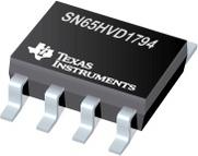
●These devices are designed to survive overvoltage faults such as direct shorts to power supplies, mis-wiring faults, connector failures, cable crushes, and tool mis-applications. They are also robust to ESD events, with high levels of protection to human-body model specifications.
●These devices combine a differential driver and a differential receiver, which operate from a single power supply. The driver differential outputs and the receiver differential inputs are connected internally to for a bus port suitable for half-duplex (two-wire bus) communication. A cable invert pin (INV) allows active correction of mis-wires that may occur during installation. Upon detecting communication errors, the user can apply a logic HIGH to the INV pin, effectively inverting the polarity of the differential bus port, thereby correcting for the reversed bus wires.
●These devices feature a wide common-mode voltage range, making them suitable for multi-point applications over long cable runs. These devices are characterized from –40°C to 105°C.
●For similar features with 3.3 V supply operation, see the SN65HVD1781 (SLLS877).
● Bus-Pin Fault Protection to > ±70 V
● Cable Invert Function Allows Correction for Reversed Bus Pins
● Common-Mode Voltage Range (–20 V to 25 V) More Than Doubles TIA/EIA
●485 Requirement
● Bus I/O Protection
● ±16 kV JEDEC HBM Protection
● Reduced Unit Load for Up to 256 Nodes
● Failsafe Receiver for Open-Circuit, Short-Circuit and Idle-Bus Conditions
● Low Power Consumption
● ICC 5 mA Quiescent During Operation
● Power-Up, Power-Down Glitch-Free Operation


