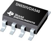
Part Datasheet Search > TI > SN65HVDA540 Datasheet PDF

 Part 3D Model
$ 0
SN65HVDA540 Datasheet PDF - TI
Manufacturer:
TI
Description:
5V CAN Transceiver With I/O Level Shifting and Supply Optimization 8-SOIC -40℃ to 125℃5
Pictures:
3D Model
Symbol
Footprint
Pinout
Product Pictures
Documentation:
SN65HVDA540 Datasheet PDF
AiEMA has not yet included the datasheet for SN65HVDA540
If necessary, please send a supplementary document request to the administrator

SN65HVDA540 Datasheet PDF (19 Pages)
SN65HVDA540 Environmental
SN65HVDA540 Function Overview
●The SN65HVDA540/SN65HVDA541 meets or exceeds the specifications of the ISO 11898 standard for use in applications employing a Controller Area Network (CAN). The device is qualified for use in automotive applications.
●As a CAN transceiver, this device provides differential transmit capability to the bus and differential receive capability to a CAN controller at signaling rates up to 1 megabit per second (Mbps)(1).
●Designed for operation in especially harsh environments, the SN65HVDA540/SN65HVDA541 features cross-wire, bus over voltage, loss of ground protection, over temperature thermal shut down protection, and a wide common-mode range.
●The SN65HVDA540/SN65HVDA541 has an I/O supply voltage input pin (VIO , pin 5) to ratiometrically level shift the digital logic input and output levels with repsect to VIO for compatibility with protocol controllers having I/O supply voltages between 3 V and 5.25 V. The VIO supply also powers the low-power bus monitor and wake-up receiver of the SN65HVDA541 allowing the 5 V (VCC) supply to be switched off for additional power savings at the system level during standby mode for either the SN65HVDA540 or SN65HVDA541. The 5 V (VCC) supply needs to be reactivated by the local protocol controller at any time to resume high speed operation if it has been turned off for low-power standby operation. Both of the supply pins have undervoltage detection which place the device in standby mode to protect the bus during an undervoltage event on either the VCC or VIO supply pins. If VIO is undervoltage the RXD pin is 3-statedn and the device does not pass any wake-up signals from the bus to the RXD pin.
●STB (pin 8) provides for two different modes of operation: normal mode or low-power standby mode. The normal mode of operation is selected by applying a low logic level to STB. If a high logic level is applied to STB, the device enters standby mode (see Figure 1 and Figure 2). In standby mode, the SN65HVDA541 provides a wake-up receiver and monitor that remains active supplied via the VIO pin so that VCC may be removed allowing a system level reduction in standby current. A dominant signal on the bus longer than the wake-up signal time (tBUS) is passed to the receiver output (RXD, pin 4) by the wake-up bus monitor circuit. The local protocol controller may then return the device to normal mode when the system needs to transmit or fully monitor the messages on the bus. If the bus has a fault condition where it is stuck dominant while the SN65HVDA541 is placed into standby mode, the device locks out the wake-up receiver output to RXD until the fault has been removed to prevent false wake-up signals in the system. Because the SN65HVDA540 does not have a low-power bus monitor and wake-up receiver, it provides a logic high output (recessive) on RXD while in standby mode.
●A dominant time-out circuit prevents the driver from blocking network communication in event of a hardware or software failure. The dominant time out circuit is triggered by a falling edge on TXD (pin 1). If no rising edge is seen before the time-out constant of the circuit expires, the driver is disabled. The circuit is reset by the next rising edge on TXD.
● Qualified for Automotive Applications
● Meets or Exceeds the Requirements of ISO 11898
● GIFT/ICT Compliant
● ESD Protection up to ±12 kV (Human-Body Model)
●on Bus Pins
● Level Adapting I/O Voltage Range to Support MCUs
●With Digital I/Os From 3 V to 5.25 V
● Low-Power Standby Mode <15 µA max
● SN65HVDA540: No Wake Up
● SN65HVDA541: Wake Up Powered By VIO
●Supply So VCC (5 V) Supply May Be Shut
●Down to Save System Power
● High Electromagnetic Immunity (EMI)
● Low Electromagnetic Emissions (EME)
● Protection
● Undervoltage Protection on VIO and VCC
● Bus-Fault Protection of 27 V to 40 V
● Dominant Time-Out Function
● Thermal Shutdown Protection
● Power-Up/Down Glitch-Free Bus Inputs and Outputs
● APPLICATIONS
● SAE J2284 High-Speed CAN for Automotive Applications
● SAE J1939 Standard Data Bus Interface
● ISO 11783 Standard Data Bus Interface
● NMEA 2000 Standard Data Bus Interface
●(1) The signaling rate of a line is the number of voltage transitions that are made per second, expressed in the units bps (bits per second).
show more
SN65HVDA540 Documents
SN65 Documents
TI
TEXAS INSTRUMENTS SN65HVD3082EDR RS485 Transceiver IC, 1 Driver, 200Kbps, 4.5V to 5.5V, SOIC-8
TI
TEXAS INSTRUMENTS SN65HVD1050DR CAN Bus, Transceiver, CAN, 1, 1, 4.5V, 5.5V, SOIC
TI
RS-485 Half-Duplex RS-485 Transceiver Single Transmitter/Receiver RS-485 8Pin SOIC T/R
TI
RS-485 Low-Power RS-485 Transceiver Single Transmitter/Receiver RS-485 8Pin SOIC Tube
Part Datasheet PDF Search
Example: STM32F103
Loading...
72,405,303 Parts Datasheet PDF, Update more than 5,000 PDF files ervery day.
BOM Matching ToolUpload BOM File
Matching parts
Alternative parts
Warning risks
Computing costs
File format: *.xlsx, *.xls, *.csv
Online 3D Gerber ViewerUpload Gerber File
Modeling in 15s
Preview PCB
40 types of layers
Preflight Risk
Support standard RS-274X file, accept zip rar or 7z
