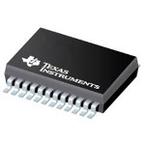
●These devices consist of bus-transceiver circuits, D-type flip-flops, and control circuitry arranged for multiplexed transmission of data directly from the input bus or from the internal registers. Data on the A or B bus is clocked into the registers on the low-to-high transition of the appropriate clock (CLKAB or CLKBA) input. Figure 1 illustrates the four fundamental bus-management functions that can be performed with the ABT646A devices.
●Output-enable (OE\\\\) and direction-control (DIR) inputs are provided to control the transceiver functions. In the transceiver mode, data present at the high-impedance port can be stored in either register or in both.
●The select-control (SAB and SBA) inputs can multiplex stored and real-time (transparent mode) data. The direction control (DIR) determines which bus receives data when OE\ is low. In the isolation mode (OE\ high), A data can be stored in one register and/or B data can be stored in the other register.
●When an output function is disabled, the input function still is enabled and can be used to store and transmit data. Only one of the two buses, A or B, can be driven at a time.
●These devices are fully specified for partial-power-down applications using Ioff. The Ioff circuitry disables the outputs, preventing damaging current backflow through the devices when they are powered down.
●To ensure the high-impedance state during power up or power down, OE\ should be tied to VCC through a pullup resistor; the minimum value of the resistor is determined by the current-sinking capability of the driver.

 Part 3D Model
