●These devices consist of bus transceiver circuits, D-type flip-flops, and control circuitry arranged for multiplexed transmission of data directly from the input bus or from the internal registers. Data on the A or B bus is clocked into the registers on the low-to-high transition of the appropriate clock (CLKAB or CLKBA) input. Figure 1 illustrates the four fundamental bus-management functions that can be performed with the ´ABT646.
●Output-enable () and direction-control (DIR) inputs are provided to control the transceiver functions. In the transceiver mode, data present at the high-impedance port may be stored in either register or in both.
●The select-control (SAB and SBA) inputs can multiplex stored and real-time (transparent mode) data. The direction control (DIR) determines which bus will receive data when is low. In the isolation mode ( high), A data may be stored in one register and/or B data may be stored in the other register.
●When an output function is disabled, the input function is still enabled and may be used to store and transmit data. Only one of the two buses, A or B, may be driven at a time.
●To ensure the high-impedance state during power up or power down, should be tied to VCC through a pullup resistor; the minimum value of the resistor is determined by the current-sinking capability of the driver.
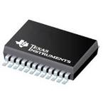
●The SN74ABT646 is available in TI"s shrink small-outline package (DB), which provides the same I/O pin count and functionality of standard small-outline packages in less than half the printed-circuit-board area.
●The SN54ABT646 is characterized for operation over the full military temperature range of -55°C to 125°C. The SN74ABT646 is characterized for operation from -40°C to 85°C.

 Part 3D Model
