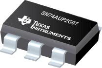
●The SN74AUP2G07 device is a dual buffer gate with open drain output that operates from 0.8 V to 3.6 V.
● Low Static-Power Consumption
●(ICC = 0.9 µA Maximum)
● Low Dynamic-Power Consumption
●pd = 1 pF
●Typical at 3.3 V)
● Low Input Capacitance (Ci = 1.5 pF Typical)
● Low Noise – Overshoot and Undershoot
●<10% of VCC
● Ioff Supports Live Insertion, Partial-Power-
●Down Mode, and Back-Drive Protection
● Input Hysteresis Allows Slow Input Transition
●and Better Switching Noise Immunity at the Input
●(Vhys = 250 mV Typ at 3.3 V)
● Wide Operating VCC Range of 0.8 V to 3.6 V
● Optimized for 3.3-V Operation
● 3.6-V I/O Tolerant to Support Mixed-Mode Signal
●Operation
● tpd = 3.3 ns Maximum at 3.3 V
● Suitable for Point-to-Point Applications
● Latch-Up Performance Exceeds 100 mA
●Per JESD 78, Class II
● ESD Performance Tested Per JESD 22
● 4500-V Human-Body Model
● 1500-V Charged-Device Model
● APPLICATIONS
● Active Noise Cancellation (ANC)
● Barcode Scanners
● Blood Pressure Monitors
● CPAP Machines
● Cable Solutions
● DLP 3D Machine Vision, Hyperspectral Imaging,
●Optical Networking, and
●Spectroscopy
● E-Books and Smartphones
● Embedded PCs
● Field Transmitters: Temperature or Pressure
●Sensor
● Fingerprint Biometrics
● HVAC: Heating, Ventilating, and Air Conditioning
● Network-Attached Storage (NAS)
● Server Motherboards and PSUs
● Software Defined Radios (SDR)
● TVs: High-Definition (HDTV), LCD, and Digital
● Video Communication Systems
● Wireless Data Access Cards, Headsets,
●Keyboards, Mice, and LAN Cards
● X-ray: Baggage Scanners, Medical, and Dental
●All other trademarks are the property of their respective owners


