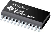
●These devices consist of bus transceiver circuits with 3-state or open-collector outputs, D-type flip-flops, and control circuitry arranged for multiplexed transmission of data directly from the input bus or from the internal registers. Data on the A or B bus will be clocked into the registers on the low-to-high transition of the appropriate clock pin (CAB or CBA). The following examples demonstrate the four fundamental bus-management functions that can be performed with the octal bus transceivers and registers.
●Enable (G\\) and direction (DIR) pins are provided to control the transceiver functions. In the transceiver mode, data present at the high-impedance port may be stored in either register or in both. The select controls (SAB and SBA) can multiplex stored and real-time (transparent mode) data. The direction control determines which bus will receive data when enable G\ is active (low). In the isolation mode (control G\ high), A data may be stored in one register and/or B data may be stored in the other register.
●When an output function is disabled, the input function is still enabled and may be used to store and transmit data. Only one of the two buses, A or B, may be driven at a time.
●The SN54" family is characterized for operation over the full military temperature range of 55°C to 125°C. The SN74" family is characterized for operation from 0° to 70°C.
● Independent Registers for A and B Buses
● Multiplexed Real-Time and Stored Data
● Choice of True or Inverting Data Paths
● Choice of 3-State or Open-Collector Outputs
● Included Among the Package Options Are Compact 24-pin 300-mil-Wide Plastic and Ceramic DIPs, Ceramic Chip Carriers, and Plastic "Small Outline" Packages
● Dependable Texas Instruments Quality and Reliability


