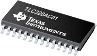
●The TLC320AC01 analog interface circuit (AIC) is an audio-band processor that provides an analog-to-digital and digital-to-analog input/output interface system on a single monolithic CMOS chip. This device integrates a band-pass switched-capacitor antialiasing input filter, a 14-bit-resolution analog-to-digital converter (ADC), a 14-bit-resolution digital-to-analog converter (DAC), a low-pass switched-capacitor output-reconstruction filter, (sin x)/x compensation, and a serial port for data and control transfers.
●The internal circuit configuration and performance parameters are determined by reading control information into the eight available data registers. The register data sets up the device for a given mode of operation and application.
●The major functions of the TLC320AC01 are: 1. To convert audio-signal data to digital format by the ADC channel 2. To provide the interface and control logic to transfer data between its serial input and output terminals and a digital signal processor (DSP) or microprocessor 3. To convert received digital data back to an audio signal through the DAC channel
●The antialiasing input low-pass filter is a switched-capacitor filter with a sixth-order elliptic characteristic. The high-pass filter is a single-pole filter to preserve low-frequency response as the low-pass filter cutoff is adjusted. There is a three-pole continuous-time filter that precedes this filter to eliminate any aliasing caused by the filter clock signal.
●The output-reconstruction switched-capacitor filter is a sixth-order elliptic transitional low-pass filter followed by a second-order (sin x)/x correction filter. This filter is followed by a three-pole continuous-time filter to eliminate images of the filter clock signal.
●The TLC320AC01 consists of two signal-processing channels, an ADC channel and a DAC channel, and the associated digital control. The two channels operate synchronously; data reception at the DAC channel and data transmission from the ADC channel occur during the same time interval. The data transfer is in2s-complement format.
●There are three basic modes of operation available: the stand-alone analog-interface mode, the master-slave mode, and the linear-codec mode. In the stand-alone mode, the TLC320AC01 generates the shift clock and frame synchronization for the data transfers and is the only AIC used. The master-slave mode has one TLC320AC01 as the master that generates the master-shift clock and frame synchronization; the remaining AICs are slaves to these signals. In the linear-codec mode, the shift clock and the frame-synchronization signals are externally generated and the timing can be any of the standard codec-timing patterns.
●Typical applications for this device include modems, speech processing, analog interface for DSPs, industrial-process control, acoustical-signal processing, spectral analysis, data acquisition, and instrumentation recorders.
●The TLC320AC01C is characterized for operation from 0°C to 70°C.
● General-Purpose Signal-Processing Analog Front End (AFE)
● Single 5-V Power Supply
● Power Dissipation . . . 100 mW Typ
● Signal-to-Distortion Ratio . . . 70 dB Typ
● Programmable Filter Bandwidths (Up to 10.8 kHz) and Synchronous ADC and DAC Sampling
● Serial-Port Interface
● Monitor Output With Programmable Gains of 0 dB, \x968 dB, \x96 18 dB, and Squelch
● Two Sets of Differential Inputs With Programmable Gains of 0 dB, 6 dB, 12 dB, and Squelch
● Differential or Single-Ended Analog Output With Programmable Gains of 0 dB, \x966 dB, \x96 12 dB, and Squelch
● Differential Outputs Drive 3-V Peak Into a 600- Differential Load
● Differential Architecture Throughout
● 1-um Advanced LinEPICTM Process
● 14-Bit Dynamic-Range ADC and DAC
● 2s-Complement Data Format
● Application Report Available
●The TLC320AC01 is functionally equivalent to the TLC320AC02 and differs in the electrical specifications as shown in Appendix C.
●Designing with the TLC320AC01 Analog Interface for DSPs (SLAA006)
●LinEPIC is a trademark of Texas Instruments Incorporated.

 Part 3D Model
