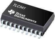
●The TLC540 and TLC541 are CMOS A/ D converters built around an 8-bit switched-capacitor successive-approximation A/D converters. They are designed for serial interface to a microprocessor or peripheral via a 3-state output with up to four control inputs, including independent SYSTEM CLOCK, I/O CLOCK, chip select (CS\\), and ADDRESS INPUT. A 4-MHz system clock for the TLC540 and a 2.1-MHz system clock for the TLC541 with a design that includes simultaneous read/write operation allow high-speed data transfers and sample rates of up to 75,180 samples per second for the TLC540 and 40,000 samples per second for the TLC541. In addition to the high-speed converter and versatile control logic, there is an on-chip 12-channel analog multiplexer that can be used to sample any one of 11 inputs or an internal self-test voltage, and a sample-and-hold that can operate automatically or under microprocessor control.
●The converters incorporated in the TLC540 and TLC541 feature differential high-impedance reference inputs that facilitate ratiometric conversion, scaling, and analog circuitry isolation from logic and supply noises. A switched-capacitor design allows low-error (±0.5 LSB) conversion in 9 us for the TLC540 and 17 us for the TLC541 over the full operating temperature range.
●The TLC540I and TLC541I are characterized for operation from \x9640°C to 85°C. The TLC541M is characterized for operation from \x9655°C to 125°C.
● 8-Bit Resolution A/D Converter
● Microprocessor Peripheral or Stand-Alone Operation
● On-Chip 12-Channel Analog Multiplexer
● Built-In Self-Test Mode
● Software-Controllable Sample and Hold
● Total Unadjusted Error ... ±0.5 LSB Max
● TLC541 Is Direct Replacement for Motorola MC145040 and National Semiconductor ADC0811. TLC540 Is Capable of Higher Speed
● Pinout and Control Signals Compatible With TLC1540 Family of 10-Bit A/D Converters
● CMOS Technology


