Web Analytics
Part Datasheet Search > - > TLC272 Datasheet PDF
Images are for reference

TLC272 Datasheet PDF

Part Series:
TLC272 Series
Category:
-
Description:
Dual Single Supply Operational Amplifier
Updated Time: 2023/01/13 01:30:29 (UTC + 8)

TLC272 Datasheet PDF -

56 Pages
TI
TEXAS INSTRUMENTS TLC272CDR Operational Amplifier, Dual, 2 Amplifier, 1.7MHz, 3.6V/µs, 3V to 16V, SOIC, 8Pins
56 Pages
TI
TEXAS INSTRUMENTS TLC272ACDR Operational Amplifier, Dual, 2 Amplifier, 1.7MHz, 3.6V/µs, 3V to 16V, SOIC, 8Pins
56 Pages
TI
TEXAS INSTRUMENTS TLC272BCDR Operational Amplifier, Dual, 2 Amplifier, 1.7MHz, 3.6V/µs, 3V to 16V, SOIC, 8Pins
56 Pages
TI
TEXAS INSTRUMENTS TLC272AID Operational Amplifier, Dual, 2 Amplifier, 1.7MHz, 3.6V/µs, 4V to 16V, SOIC, 8Pins
56 Pages
TI
Operational Amplifier, Dual, 2 Amplifier, 1.3MHz, 3.6V/µs, 3V to 16V, SOIC, 8Pins
56 Pages
TI
TEXAS INSTRUMENTS TLC272IP Operational Amplifier, Dual, 2 Amplifier, 1.7MHz, 3.6V/µs, 4V to 16V, DIP, 8Pins
56 Pages
TI
TEXAS INSTRUMENTS TLC272ACD Operational Amplifier, Dual, 2 Amplifier, 1.7MHz, 3.6V/µs, 3V to 16V, SOIC, 8Pins
56 Pages
TI
TEXAS INSTRUMENTS TLC272ACP Operational Amplifier, Dual, 2 Amplifier, 1.7MHz, 3.6V/µs, 3V to 16V, DIP, 8Pins
56 Pages
TI
TEXAS INSTRUMENTS TLC272CPW Operational Amplifier, 2 Amplifier, 2.2MHz, 5.3V/µs, 3V to 16V, TSSOP, 8Pins
53 Pages
TI
Operational Amplifier, Dual, 2 Amplifier, 1.7MHz, 3.6V/µs, 4V to 16V, SOIC, 8Pins
53 Pages
TI
TEXAS INSTRUMENTS TLC272BCD Operational Amplifier, Dual, 2 Amplifier, 1.7MHz, 3.6V/µs, 3V to 16V, SOIC, 8Pins
53 Pages
TI
TEXAS INSTRUMENTS TLC272ID Operational Amplifier, Dual, 2 Amplifier, 2.6MHz, 3.6V/µs, 4V to 16V, SOIC, 8Pins
53 Pages
TI
TEXAS INSTRUMENTS TLC272BCP Operational Amplifier, 2 Amplifier, 2.2MHz, 5.3V/µs, 3V to 16V, DIP, 8Pins
53 Pages
TI
Standard Linear AmplifierLinCMOS<TM> Precision Dual Operational Amplifier Op Amp Dual GP 16V 8Pin SOIC T/R
53 Pages
TI
Op Amp Dual GP 16V 8Pin PDIP Tube
53 Pages
TI
Dual Single Supply Operational Amplifier

TLC272 Function Overview

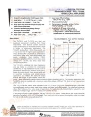
The TLC272 and TLC277 precision dual operational amplifiers combine a wide range of input offset voltage grades with low offset voltage drift, high input impedance, low noise, and speeds approaching those of general-purpose BiFET devices.
These devices use Texas Instruments silicon-gate LinCMOS™ technology, which provides offset voltage stability far exceeding the stability available with conventional metal-gate processes.
The extremely high input impedance, low bias currents, and high slew rates make these cost-effective devices ideal for applications previously reserved for BiFET and NFET products. Four offset voltage grades are available (C-suffix and I-suffix types), ranging from the low-cost TLC272 (10 mV) to the high-precision TLC277 (500 uV). These advantages, in combination with good common-mode rejection and supply voltage rejection, make these devices a good choice for new state-of-the-art designs as well as for upgrading existing designs.
In general, many features associated with bipolar technology are available on LinCMOS™ operational amplifiers without the power penalties of bipolar technology. General applications such as transducer interfacing, analog calculations, amplifier blocks, active filters, and signal buffering are easily designed with the TLC272 and TLC277. The devices also exhibit low voltage single-supply operation, making them ideally suited for remote and inaccessible battery-powered applications. The common-mode input voltage range includes the negative rail.
A wide range of packaging options is available, including small-outline and chip carrier versions for high-density system applications.
The device inputs and outputs are designed to withstand –100-mA surge currents without sustaining latch-up.
The TLC272 and TLC277 incorporate internal ESD-protection circuits that prevent functional failures at voltages up to 2000 V as tested under MIL-STD-883C, Method 3015.2; however, care should be exercised in handling these devices as exposure to ESD may result in the degradation of the device parametric performance.
The C-suffix devices are characterized for operation from 0°C to 70°C. The I-suffix devices are characterized for operation from –40°C to 85°C. The M-suffix devices are characterized for operation over the full military temperature range of –55°C to 125°C.
Trimmed Offset Voltage:
       TLC277 . . . 500 uV Max at 25°C, VDD = 5 V
Input Offset Voltage Drift ...Typically 0.1 uV/Month, Including the First 30 Days
Wide Range of Supply Voltages Over Specified Temperature Range:
       0°C to 70°C ...3 V to 16 V
       –40°C to 85°C ...4 V to 16 V
       –55°C to 125°C ...4 V to 16 V
Single-Supply Operation
Common-Mode Input Voltage Range Extends Below the Negative Rail (C-Suffix, I-Suffix types)
Low Noise ...Typically 25 nV/Hz at f = 1 kHz
Output Voltage Range Includes Negative Rail
High Input impedance ...1012 Typ
ESD-Protection Circuitry
Small-Outline Package Option Also Available in Tape and Reel
Designed-In Latch-Up Immunity
LinCMOS is a trademark of Texas Instruments.
show more
Part Datasheet PDF Search
Loading...
72,405,303 Parts Datasheet PDF, Update more than 5,000 PDF files ervery day.
Relate Parts