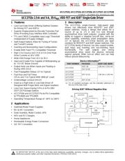
●The UCC2753x single-channel, high-speed gate drivers can effectively drive MOSFET and IGBT power switches. Using a design that allows for a source of up to 2.5 A and 5-A sink through asymmetrical drive (split outputs), coupled with the ability to support a negative turn-off bias, rail-to-rail drive capability, extremely small propagation delay (17 ns typical), the UCC2753x devices are ideal solutions for MOSFET and IGBT power switches. The UCC2753x family of devices can also support enable, dual input, and inverting and non-inverting input functionality. The split outputs and strong asymmetrical drive boost the devices immunity against parasitic Miller turn-on effect and can help reduce ground debouncing.
●Leaving the input pin open holds the driver output low. The logic behavior of the driver is shown in the application diagram, timing diagram, and input and output logic truth table.
●Internal circuitry on VDD pin provides an undervoltage lockout function that holds output low until VDD supply voltage is within operating range.
● Low-Cost Gate Driver (Offering Optimal Solution
●for Driving FET and IGBTs)
● Superior Replacement to Discrete Transistor Pair
●Drive (Providing Easy Interface With Controller)
● TTL and CMOS Compatible Input Logic Threshold
●(Independent of Supply Voltage)
● Split Output Options Allow for Tuning of Turnon
●and Turnoff Currents
● Inverting and Noninverting Input Configurations
● Enable With Fixed TTL Compatible Threshold
● High 2.5-A Source and 2.5-A or 5-A Sink Peak
●Drive Currents at 18-V VDD
● Wide VDD Range From 10 V to 35 V
● Input and Enable Pins Capable of Withstanding up
●to –5-V DC Below Ground
● Output Held Low When Inputs are Floating or
●During VDD UVLO
● Fast Propagation Delays (17-ns Typical)
● Fast Rise and Fall Times
●(15-ns and 7-ns Typical With 1800-pF Load)
● Undervoltage Lockout (UVLO)
● Used as a High-Side or Low-Side Driver (If
●Designed With Proper BIAS and Signal Isolation)
● Low-Cost, Space-Saving 5-Pin or 6-Pin DBV
●(SOT-23) Package Options
● UCC27536 and UCC27537 Pin-to-Pin Compatible to
●TPS2828 and TPS2829
● Operating Temperature Range of –40°C to 140°C