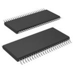
●This 16-bit bus transceiver and register is designed for 1.65-V to 3.6-V VCC operation.
●The SN74LVCH16646A can be used as two 8-bit transceivers or one 16-bit transceiver. The device consists of bus transceiver circuits, D-type flip-flops, and control circuitry arranged for multiplexed transmission of data directly from the input bus or from the internal registers.
●Data on the A or B bus is clocked into the registers on the low-to-high transition of the appropriate clock (CLKAB or CLKBA) input. Figure 1 illustrates the four fundamental bus-management functions that can be performed with the SN74LVCH16646A.
●Output-enable (OE)\ and direction-control (DIR) inputs control the transceiver functions. In the transceiver mode, data present at the high-impedance port can be stored in either register or in both. The select-control (SAB and SBA) inputs can multiplex stored and real-time (transparent mode) data. The circuitry used for select control eliminates the typical decoding glitch that occurs in a multiplexer during the transition between stored and real-time data. DIR determines which bus receives data when OE\ is low. In the isolation mode (OE\ high), A data can be stored in one register and/or B data can be stored in the other register.
●This device is fully specified for partial-power-down applications using Ioff. The Ioff circuitry disables the outputs, preventing damaging current backflow through the device when it is powered down.
●When an output function is disabled, the input function is still enabled and can be used to store and transmit data. Only one of the two buses, A or B, can be driven at a time.
●Inputs can be driven from either 3.3-V or 5-V devices. This feature allows the use of these devices as translators in a mixed 3.3-V/5-V system environment.
●To ensure the high-impedance state during power up or power down, OE\ should be tied to VCC through a pullup resistor; the minimum value of the resistor is determined by the current-sinking capability of the driver.
●Active bus-hold circuitry holds unused or undriven inputs at a valid logic state. Use of pullup or pulldown resistors with the bus-hold circuitry is not recommended.

 Part 3D Model
